
Return to main page
Background for beginners
What I did last summer
Skills and Experiences
More info (for experts/collaborators)
What's next?
Philippa Young
Designing an Analogue Low Pass Filter System for a Quantum Ion Trap.
Designing the PCB and sourcing parts
Once you have a circuit diagram such as the ones output by the filter simulation packages you need to convert the chosen design to a PCB layout.
For this I used a program called Novarm Dip Trace. There are many programs which can be used but this was the only one I found with the capability to do all the required surface mounted components.
For a quick explanation of how to use this program click here.
The PCB for an active filter can be seen in the following diagram. As predicted the circuit is quite complex and therefore has a large area.
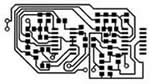
The PCB for a passive filter is much more compact as can be seen below.
![]()
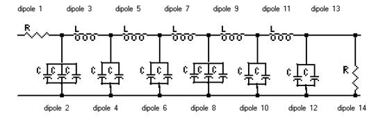
The filter we are going to use is the Chebyshev type I 11th order. The circuit diagram and parts values can be seen below.
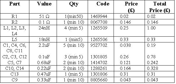
The PCB for this filter is extremely small; I have used surface mounted components in 0805 casing which are roughly 2mm long. This will allow a large number of filters to be placed on one circuit board.
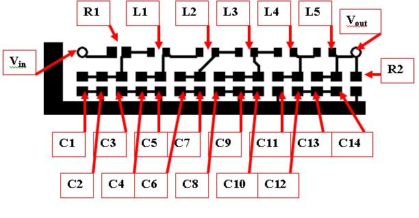
The following diagram is labeled with the part code I have assigned to each component. These correspond to the parts in the part list above.
The values for the parts were selected by looking at which values were available to us in the 0805 casing, in order to optimise the curve I have used several capacitors in parallel to get as close as possible to the optimum curve.