Return to main page
Background for beginners
What I did last summer
Skills and Experiences
More info (for experts/collaborators)
What's next?
Philippa Young
Designing an Analogue Low Pass Filter System for a Quantum Ion Trap.
Manufacturing
PCB manufacture
Manufacturing a test filter is done by printing the PCB onto a transparency and using photoresist copper clad board.
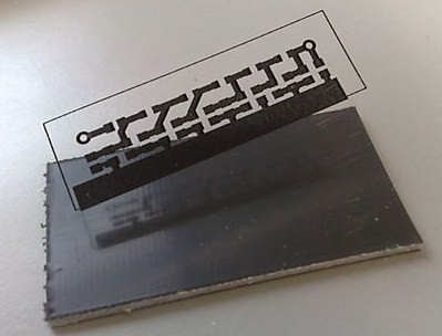
(Photo showing the piece of PCB board cut to size and the printed transparency)
You place the design onto the copper board and expose it to several minutes of UV light, this causes a change in the photoresist coating on the PCB.
When the exposed PCB is placed into a developing solution the copper tracks will appear a green/blue colour and the rest of the PCB will remain copper coloured.
The PCB is then rinsed with water and placed into an etching solution which will eat away all the unneeded copper; leaving behind just the copper tracks and pads.
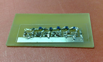
Soldering the components
Once the PCB is made and has been cleaned to remove the green layer of photoresist, the components can be soldered on. The surface mount components are soldered directly to the pads on the PCB.
Small holes will need to be drilled for the Vin and Vout wires to be attached.
A ground has to be attached to the large copper filled area.
The PCB can then be tested before a full board of 100 is made.